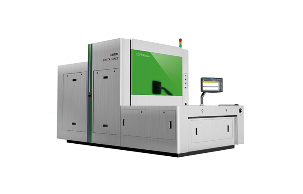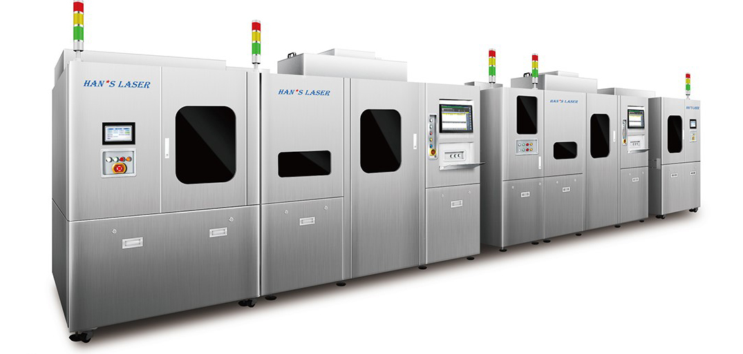
★ Independent high laser energy DMD control technology, enhance the reliability of equipment
★ With high quality and high power composite wavelength light source, enhance the polymerization efficiency of solder mask
★ Exposure process is all digital operation, enter the industry 4.0 intelligent manufacturing
Maximum exposure size
Large table: 24.5"×28.5"
Standard table: 22"×24.5"
Resistance welding open the window
75 microns
The light source
Composite wavelength
Panel thickness
Single machine: 0.05 - 5.0 mm
In-line: 0.1 - 3.5 mm
The depth of field
±300μm
Line width precision
±10%
Registration accuracy
±12μm
Fitment
Suitable for intelligent manufacturing systems
Soder mask bridge capability
50 microns
